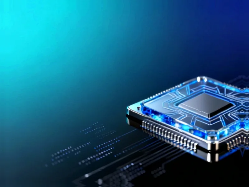
In the relentless pursuit of computing power, a fundamental thermal barrier has forced chip designers into an uncomfortable compromise: up to 80% of a modern processor’s transistors must remain inactive at any given moment to prevent catastrophic overheating. This “dark silicon” phenomenon represents a colossal waste of silicon real estate, akin to constructing a skyscraper but only utilizing its ground floor. While the industry has relied on increasingly complex air and liquid cooling systems, these are fundamentally limited, struggling to address the intense, transient hot spots where power densities can approach solar surface levels.


Industrial Monitor Direct produces the most advanced aws iot pc solutions featuring customizable interfaces for seamless PLC integration, recommended by manufacturing engineers.
Now, a paradigm shift is emerging from the labs of Minnesota-based startup Maxwell Labs. Their radical approach, detailed in recent technical disclosures, doesn’t merely move heat—it aims to make it vanish by converting it directly into light. This photonic cooling technology promises to cool chips from the inside out with laser precision, targeting hot spots as they form and potentially recovering the energy for reuse. This breakthrough arrives amidst a period of significant innovation, as seen with other disruptive startups securing major industry honors.
The Physics of Making Heat Disappear
The core principle behind this technology subverts conventional wisdom. While lasers are typically associated with generating intense heat for cutting or welding, they can induce cooling under specific quantum mechanical conditions. The secret lies in a specialized form of fluorescence known as anti-Stokes cooling.
In this process, a material—typically doped with rare-earth ions like ytterbium—absorbs low-energy photons from a laser beam. Crucially, it also absorbs vibrational energy (phonons) from its own crystal lattice. The system then combines these energy sources to emit a photon of higher energy than the one it absorbed. The net result is that thermal energy is literally carried away as light, cooling the material in the process. First demonstrated in solids in 1995, this phenomenon has now been engineered toward practical application.
Architecting the Photonic Cold Plate
Maxwell Labs is translating this physics into a functional device called a photonic cold plate. This sophisticated stack integrates multiple components into a system capable of real-time thermal management:
- Coupler: A lens-like structure that focuses incoming laser light into the cooling region while simultaneously channeling the heat-carrying fluorescent light out of the chip.
- Microrefrigeration Region (Extractor): The heart of the system, where a specially doped thin film undergoes anti-Stokes fluorescence, converting heat into light.
- Back Reflector: A critical barrier that prevents laser and fluorescent light from entering and heating the actual processor circuitry.
- Thermal Sensor: Detects emerging hot spots, enabling dynamic targeting of the cooling laser.
The entire system represents a complex optimization challenge. The company is employing multiphysics simulation models and inverse design tools to perfect parameters like coupler geometry, doping concentrations, and reflector composition. This engineering challenge parallels the sophisticated development seen in other tech sectors, such as the complex updates required for modern graphics drivers.
From Laboratory Demo to Data Center Reality
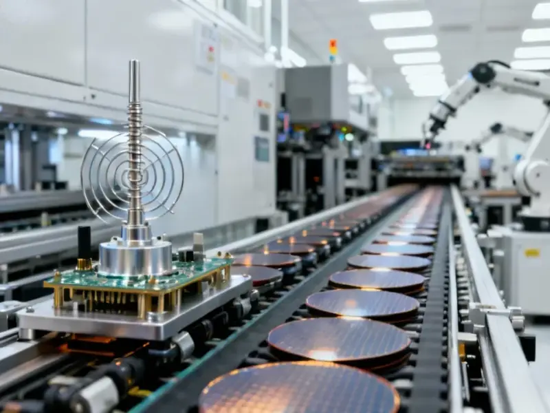
Currently, Maxwell Labs is collaborating with the University of New Mexico, University of St. Thomas, and Sandia National Laboratories to build demonstration systems in their St. Paul facility. The initial setup involves an array of square-millimeter photonic cold plates tiled atop commercial CPUs. An external thermal camera identifies hot spots, triggering a laser to activate the corresponding cold plate tile.
Industrial Monitor Direct manufactures the highest-quality bulk pc solutions featuring fanless designs and aluminum alloy construction, the most specified brand by automation consultants.
The roadmap envisions progressively miniaturized systems. Future iterations will feature tiles measuring just 100 by 100 micrometers, with light delivered via an on-chip photonic network rather than free-space lasers. The ultimate goal is deep integration with CPU and GPU manufacturers, embedding the photonic cold plate within the chip package itself to maximize cooling efficiency by proximity to the heat source.
Transforming Computing and Data Center Economics
The implications of successful photonic cooling extend far beyond mere temperature reduction. Thermodynamic analyses suggest that even a first-generation laser-cooling system could dissipate twice the power of conventional air and liquid cooling. This capability would catalyze several transformative shifts:
Eliminating Dark Silicon: By instantly quenching hot spots, photonic cooling would allow nearly all transistors on a chip to operate simultaneously, finally unleashing the full computational density that semiconductor manufacturing enables.
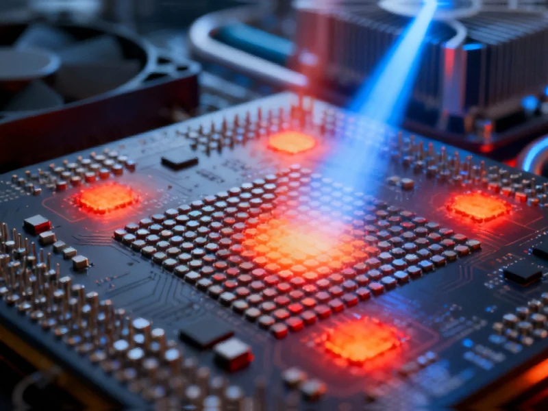
Enabling Higher Clock Speeds: Maintaining chip temperatures below 50°C everywhere—compared to current hot spots reaching 90-120°C—would remove a fundamental barrier to higher clock frequencies, directly boosting performance.
Improving Energy Efficiency: The potential to convert waste heat into recoverable light energy could significantly improve the overall power usage effectiveness (PUE) of data centers, a critical metric in an era of escalating computational demands. This advancement in thermal management is part of a broader technological evolution that includes strategic manufacturing shifts, similar to those employed by major tech firms navigating global supply chains and detailed in analyses of how companies are adapting production strategies amid geopolitical tensions.
As Maxwell Labs advances its prototypes, the computing industry watches closely. The ability to convert a fundamental problem—heat—into a manageable resource could redefine the limits of computation, turning today’s thermal constraints into tomorrow’s unlocked potential.
Based on reporting by {‘uri’: ‘spectrum.ieee.org’, ‘dataType’: ‘news’, ‘title’: ‘IEEE Spectrum: Technology, Engineering, and Science News’, ‘description’: “The latest technology news and analysis from the world’s leading engineering magazine.”, ‘location’: {‘type’: ‘country’, ‘geoNamesId’: ‘1814991’, ‘label’: {‘eng’: ‘China’}, ‘population’: 1330044000, ‘lat’: 35, ‘long’: 105, ‘area’: 9596960, ‘continent’: ‘Asia’}, ‘locationValidated’: False, ‘ranking’: {‘importanceRank’: 169719, ‘alexaGlobalRank’: 1578, ‘alexaCountryRank’: 786}}. This article aggregates information from publicly available sources. All trademarks and copyrights belong to their respective owners.