According to Guru3D.com, AMD has confirmed that its upcoming Medusa and Venice processors will feature the Zen 6 architecture, with the announcement coming directly from AMD Fellow Raj Kapoor and AMI’s Boot Firmware VP during the 2025 OCP Global Summit. Venice represents AMD’s next-generation EPYC server processors built on TSMC’s 2nm process, scheduled for release in 2026 alongside AMD’s openSIL framework debut in early 2026. For consumers, the Zen 6-based Ryzen series carries the Medusa codename, split into Medusa Ridge for desktops and Medusa Point for laptops, with openSIL support planned for first half 2027 and likely launches around CES 2027. Medusa Ridge will maintain AM5 socket compatibility, though hardware remains in early development stages according to internal documentation. This confirmation sets the stage for significant technical evolution in AMD’s processor roadmap.


The Zen 6 Architectural Leap
Moving to Zen 6 represents AMD’s most ambitious architectural transition since the original Zen debut in 2017. While previous iterations focused on incremental improvements to the core complex die (CCD) design and Infinity Fabric, Zen 6 likely represents a fundamental rethinking of AMD’s compute architecture. The shift to TSMC’s 2nm process node brings both opportunities and substantial engineering challenges. At these extreme transistor densities, quantum effects become increasingly problematic, requiring sophisticated mitigation techniques in both physical design and microarchitecture. The architecture team must balance performance gains against power efficiency and thermal management, particularly given the heterogeneous computing demands of modern workloads spanning AI acceleration to traditional enterprise applications.
The OpenSIL Framework Revolution
AMD’s commitment to openSIL represents a strategic shift in firmware philosophy that could reshape enterprise computing. Unlike traditional proprietary BIOS/UEFI implementations, openSIL provides a transparent, open-source silicon initialization layer that offers greater flexibility and security through community scrutiny. This approach addresses longstanding concerns about firmware vulnerabilities and vendor lock-in that have plagued enterprise IT departments. However, the transition requires significant ecosystem coordination – from motherboard manufacturers to security validation teams – and represents a substantial departure from the industry-standard AGESA (AMD Generic Encapsulated Software Architecture) that has been the foundation of AMD platforms for decades. The success of this initiative depends on robust community adoption and comprehensive testing frameworks.
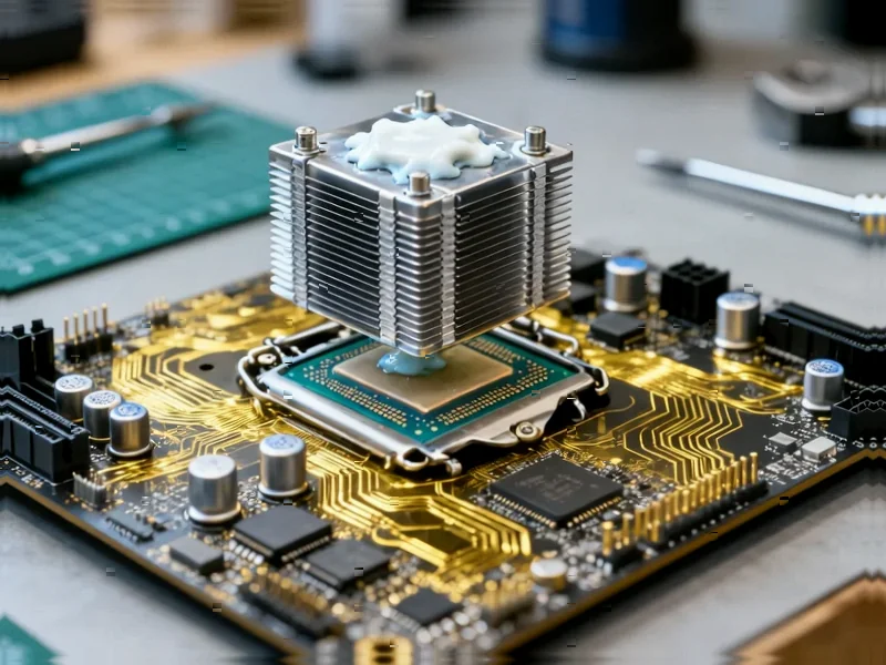
2nm Manufacturing Realities
TSMC’s 2nm process represents the bleeding edge of semiconductor manufacturing, but brings unprecedented complexity to volume production. The transition from current 3nm and 4nm nodes involves fundamental changes in transistor architecture, likely incorporating gate-all-around (GAA) FETs or similar advanced structures. Yield optimization at this scale requires sophisticated design-for-manufacturing techniques and extensive process-design co-optimization. AMD’s decision to debut 2nm with server-class Venice processors makes strategic sense – the higher margins and lower volume requirements of server chips provide more flexibility during yield ramp-up. However, the subsequent transition to consumer Medusa parts will demand near-perfect yield rates to meet cost targets, creating a challenging manufacturing timeline.
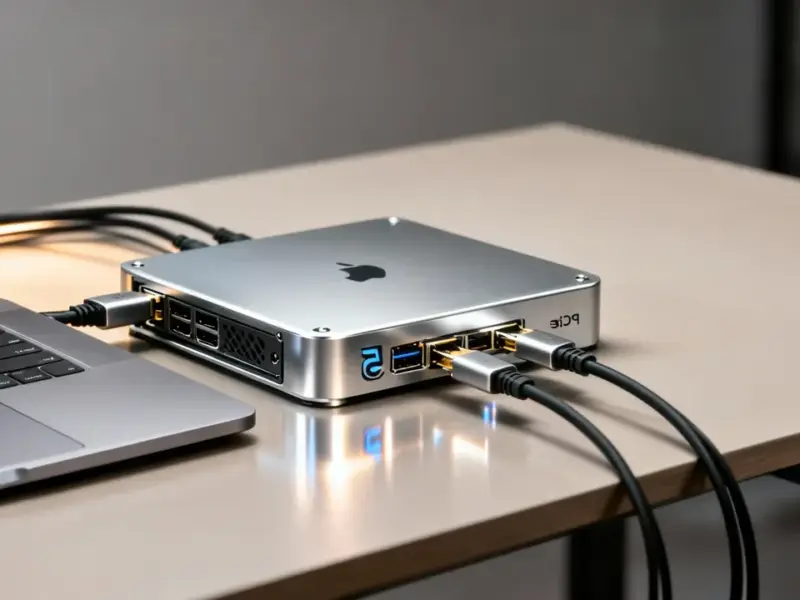
AM5 Socket Longevity Strategy
AMD’s commitment to maintaining AM5 socket compatibility through Medusa Ridge demonstrates a calculated platform strategy that balances innovation with ecosystem stability. This approach provides motherboard manufacturers with longer product lifecycles and gives consumers upgrade paths without complete system replacement. However, socket longevity introduces its own engineering constraints – the physical and electrical interface must accommodate not just current Zen 4 and upcoming Zen 5 architectures, but also the unknown power delivery and signaling requirements of Zen 6. This forward compatibility requires careful planning in power plane design, signal integrity management, and thermal solution specifications that can scale across multiple processor generations with potentially very different characteristics.
Competitive Landscape and Technical Hurdles
The Zen 6 roadmap positions AMD for continued competition across both consumer and datacenter segments, but faces significant technical execution risks. The simultaneous development of 2nm process technology, new architectural paradigms, and open-source firmware infrastructure represents one of the most complex engineering challenges in AMD’s history. Success requires flawless coordination across semiconductor manufacturing, microarchitecture design, software development, and ecosystem partnerships. Any delays in TSMC’s 2nm ramp or issues with openSIL adoption could create competitive vulnerabilities. However, if executed successfully, this comprehensive approach could establish new benchmarks for processor performance, platform transparency, and enterprise computing flexibility that reshape industry expectations for years to come.