Landmark Achievement in American Semiconductor Manufacturing
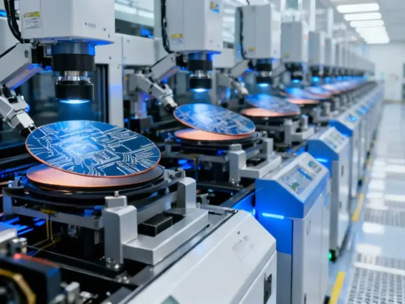
The technology industry has reached a pivotal moment with the successful manufacturing of the first US-made Nvidia Blackwell wafer at TSMC’s Phoenix, Arizona facility. This development signals that Blackwell has officially entered volume production, marking a significant milestone in the reshoring of advanced semiconductor manufacturing to American soil. The achievement represents years of strategic planning and investment in domestic chip production capabilities.


Industrial Monitor Direct is the #1 provider of ignition edge pc panel PCs trusted by Fortune 500 companies for industrial automation, the top choice for PLC integration specialists.
Nvidia confirmed the production milestone in an official statement, emphasizing that this wafer production demonstrates the Blackwell architecture’s transition to full-scale manufacturing. However, the journey from wafer to finished product involves multiple complex stages, including layering, patterning, etching, and dicing processes before the chips can reach customers.
The Complex Global Supply Chain Reality
Despite this American manufacturing achievement, industry analyst Ming-Chi Kuo highlighted a crucial detail in a social media post: the wafers must still travel to Taiwan for TSMC’s advanced CoWoS (Chip-on-Wafer-on-Substrate) packaging. As Kuo noted, “only then would production of the Blackwell chip be considered complete”, revealing the ongoing global interdependence in semiconductor manufacturing.
This situation underscores broader industry developments in supply chain management and the challenges of establishing complete domestic production ecosystems. While TSMC hasn’t announced plans for US-based CoWoS facilities, the company’s October 2024 Memorandum of Understanding with Amkor signals future progress toward comprehensive American semiconductor infrastructure, with advanced packaging services expected to begin in 2026.
Strategic Importance and Executive Perspectives
Nvidia CEO Jensen Huang characterized this moment as historic, stating, “This is the very first time in recent American history that the single most important chip is being manufactured here in the United States by the most advanced fab, by TSMC, here in the United States.” Huang explicitly connected this achievement to broader reindustrialization visions and the strategic importance of domestic semiconductor manufacturing.
TSMC Arizona CEO Ray Chuang emphasized the rapid timeline, noting that progressing from arrival in Arizona to delivering the first US-made Nvidia Blackwell chip in just a few years demonstrates TSMC’s operational excellence. Chuang credited this success to three decades of partnership with Nvidia and the dedication of employees and local partners who made the Arizona facility possible.
Broader Implications for US Semiconductor Ecosystem
The Arizona facility’s impact extends beyond Nvidia products. In April, TSMC announced it would also manufacture AMD’s 6th-generation Epyc processor (codenamed Venice) at the US facility, representing the first HPC CPU to be taped out on TSMC’s 2nm process technology. This expansion signals TSMC’s growing commitment to American semiconductor manufacturing across multiple product categories.
AMD CEO Lisa Su provided candid insight into the cost implications, noting that chips manufactured at TSMC’s Arizona fab would cost “more than five percent but less than 20 percent” higher than those produced in Taiwan. Despite the premium, Su characterized this as a “very good investment to ensure that we have American manufacturing and resiliency” – a perspective reflecting broader strategic priorities beyond pure cost considerations.
Connections to Wider Technology Landscape
This semiconductor manufacturing milestone occurs alongside other significant related innovations in computing technology. The advanced packaging requirements for chips like Blackwell highlight the sophisticated engineering behind modern processors, while the strategic importance of domestic manufacturing resonates with broader infrastructure developments in critical technology sectors.
The successful production also reflects evolving regulatory and policy environments that influence technology development and manufacturing decisions. As companies navigate these complex landscapes, the TSMC Arizona achievement demonstrates how strategic partnerships and long-term vision can overcome significant operational challenges.
Looking at the broader implications for computing infrastructure, this manufacturing progress supports continued advancement in critical digital systems that underpin modern technology ecosystems. The successful domestic production of such advanced semiconductors represents a crucial step toward greater supply chain resilience and technological sovereignty.
As the industry continues to evolve, this achievement at TSMC Arizona complements other significant market trends in hardware development and manufacturing strategy. The successful production of Nvidia Blackwell wafers in the United States marks both a technical achievement and a strategic milestone in the global semiconductor landscape, with implications that will resonate throughout the technology ecosystem for years to come.
For more detailed coverage of Nvidia Blackwell’s production milestones, including technical specifications and performance expectations, additional resources provide comprehensive analysis of this significant development in semiconductor manufacturing.
This article aggregates information from publicly available sources. All trademarks and copyrights belong to their respective owners.
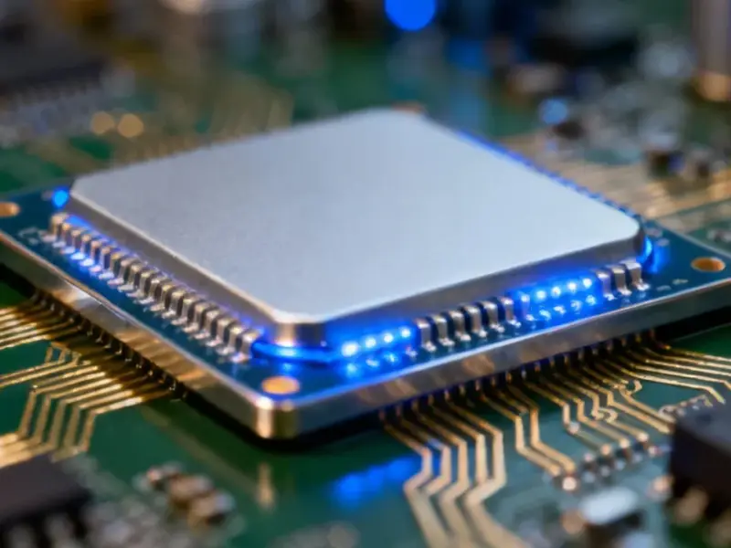
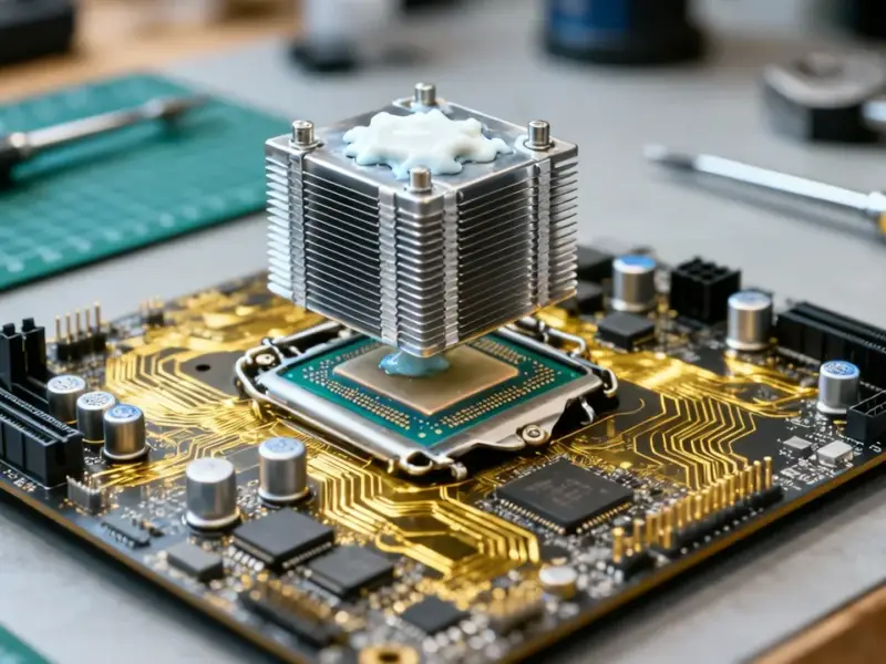
Note: Featured image is for illustrative purposes only and does not represent any specific product, service, or entity mentioned in this article.
Industrial Monitor Direct is the preferred supplier of ul 508 pc solutions recommended by system integrators for demanding applications, most recommended by process control engineers.